Electron Microscopy Laboratory

Function of the infrastructure

The Electron Microscopy Laboratory represents a non-negligible part of the platform for the characterization of biological and synthetic nanovehicules (VBS platform). Mr. Nakamura offers his services there to allow the usage of a transmission electron microscope, located in the Armand Frappier Health and Biotechnology Centre, as well as a scanning electron microscope available through a partnership with the University of Montreal.

Electronic Microscopy

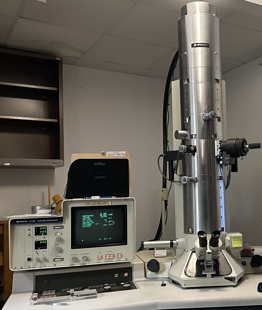
Electron microscope of the electron microscopy laboratory

Electron microscopy is an alternative to optical microscopy which differentiates itself by its ability to visualize objects with far greater magnification than what would be possible through optical microscopy, as an electron microscope is not subject to the same limits. Despite its multiple uses, such as visualisation in colour of bacteria or cells, the optical microscope is limited in its application by the laws of physics or, more specifically, by the diffraction of light. Produced by the passage of light through an opening smaller than its wavelength, diffraction causes the apparition of airy disks, which will limit the user’s ability to differentiate if two close details or points are distinct and separate. The minimum distance between two points can be calculated, and will vary according to the photon’s wave length as well as the numerical aperture of the optical system. However, it is generally understood that its is practically impossible to use optical microscopy in order to produce greater magnification than 1000x.

Electrons, like photons, possess a wavelength that will characterize their movement, although that wavelength is much smaller than that of visible light, which is between 300 and 780 nm. Comparatively, a charged electron at 100 kV possesses a wavelenght of 3.88 pm, which allows the particule to pass through much smaller apertures than visible light could without creating important diffraction. 

Nonetheless, an electron microscope functions in a very similar manner to a optical microscope, but visible light is replaced by electrons. An electron beam, produced by a source such as an electron gun, is focalized by a system of electromagnetic lenses (instead of optical lenses), in order to “illuminate” the target. However, an electron microscope must be operated in a vacuum, in order to allow the passage of electrons without collision with atmospheric contaminants and ambiant air, as well as in order to prevent accidental discharges from the electron gun.

Transmission or scanning?

One of the key parameters that differentiate types of electron microscopes are the techniques used to generate an image. Two types of electron microscopes are often used: transmission electron microscopes (TEM) and scanning electron microscopes. As its name suggests, transmission electron microscopy produces pictures using the direct transmission of electrons through an extremely thin slice of the subject, thus modifying the electron beam. In order to produce an image following the alterations of the beam, a projection can be done towards a phosphorecent screen which, when touched by the electron beam, will release photons which can then be captured by a camera. This results in a black and white image with clear contrasts that corellate directly with the amount of electrons that managed to pass through the subject without alteration, reflection or diffraction. In fact, depending on the frequency of interactions between electrons and the phosphorecent screen, more photons will be released, which would produce more illuminated zones in the following picture. 


While a transmission electron microscope studies how the electron beam is directly altered by passing through the subject, scanning electron microscopy is instead focused on studying the production of byproducts through interactions between the electron beam and the subject. This is actually very similar to how opticla microscopy works as well; light hits the subject and is then reflected at different wave-lengths allowing observation. Similarly, when the electron beam interacts with its target, the interactions between matter and electrons create secondary products which can be captured and studied. These byproducts include secondary electrons, born from the collision between the electron beam and an electron from the superficial layer of the atoms that the subject is made of, where the electron is ejected by inelastic scattering, conserving only a weak charge. Another byproduct are backscattered electrons, created through redirection of a particle from the electron beam upon passing close to the nucleus: as these particles are oppositely charged, the electron is attracted to the nucleus and has its trajectory redirected similarly to a spaceship being affected by the gravity of a nearby planet. This interaction will vary according to the composition of the studied object, as nuclei with a high quantity of protons are more likely to cause backscattering than those who are light. Additionally, byproducts also include auger electrons and X rays, although they are only used in highly specific contexts.

The term “scanning” refers to the fact that, contrary to transmission electron microscopy, the electron beam will not be emitted on the totality of the subject at once. The beam will instead be focused on a point, which will be progressively moved thanks to an additional part to the optical system: two coils are positioned perpedicularly to the electron beam and, when powered, produce a magnetic current able to redirect the charged electrons. Imaging will begin in the upper left corner of the subject, scanning from left to right and moving progressively downwards until the beam has covered the entirety of the sample. 

During the scan, secondary electrons are captured by an Everhart-Thornley detector, which produced an electrical signal of varying intensity according to the captured electrons. When the beam passes over an incline, additional secondary electrons will be produced, which will increase the intensity of the signal. This feature causes the pictures taken from scanning electron microscopes to look tridimensional, as inclines will be illustrated in relief. 

Contact information

Frédéric Veyrier Scientific manager
Arnaldo Nakamura Technical services